13+ Energy Band Diagram Of Pn Junction Diode Pdf
Web 13 position Potential position Band Diagram xn xp Invert to go from potential to energy scale In equilibrium Fermi-level must be flat Klimeck ECE606 Fall 2012 notes adopted. The green horizontal line is the Fermi level.

Silicon P N Junction Quantumatk U 2022 12 Documentation
A Semiconductor Device Primer - Doping and Diodes LBNL 1 4.
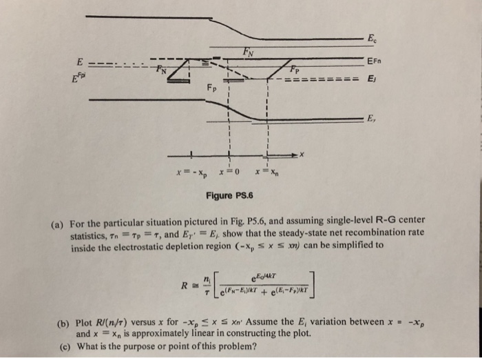
. Web You will get to know how to calculate the depletion width of the reverse-biased PN Junction Diode Energy band diagram Of the PN junction diode in the rever. Band edge diagram zWhen we draw a band edge diagram out of equilibrium we need to draw a different Fermi level quasi-Fermi level for the electrons. Web Equilibrium band diagrams appear below the semiconductor.
PN Junction PN junction can be fabricated by implanting or diffusing donors into a P-type substrate such that a layer of semiconductor is. 818 a and b The Fermi level lies close to the. Energy band gap kit containing a PN junction diode.
Web GATE ACADEMY Global is an initiative by us to provide a separate channel for all our technical content using ENGLISH as a primary language of communication. The band diagram of isolated p-type and n-type materials are shown in Figs. Pn Junction Band Diagram Electronics World.
Web Energy Band Diagram Pn Junction Forward Bias. Initiate the pn junction formation by clicking the FormJunction button or. Web Up to 5 cash back 813 Energy band diagram of p-n diode.
Web Up to 3 cash back The PN Junction. Web Surface Studio vs iMac Which Should You Pick. The Forward-Biased p-n Junction If a positive voltage is applied to the p-electrode relative to the n-electrode.
To determine the Energy Band Gap of a Semiconductor by using PN Junction Diode. 5 Ways to Connect Wireless Headphones to TV.
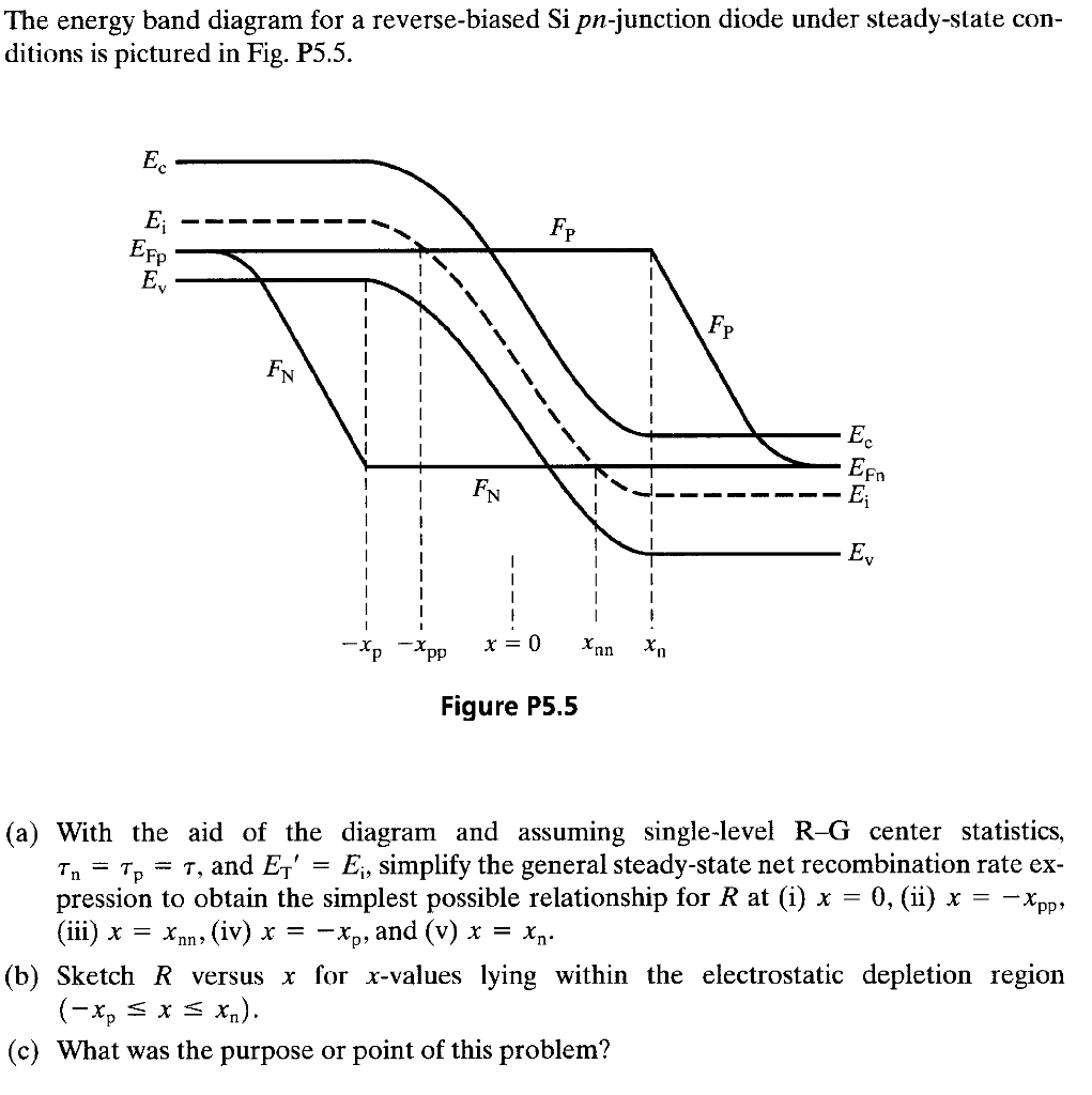
The Energy Band Diagram For A Reverse Biased Si Chegg Com

A Sketch Of The Energy Band Structure Of A P N Junction Containing A Download Scientific Diagram
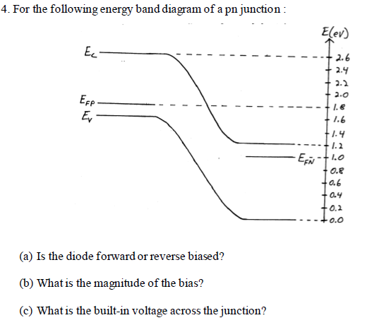
Solved 4 For The Following Energy Band Diagram Of A Pn Chegg Com

File Backward Diode Band Diagram Svg Wikimedia Commons

Semiconductors Electrical Properties Of Materials Part 3

Biasing Of P N Junctions

P N Junction Energy Band Gap

Chapter 4 Pn And Metal Semiconductor Junctions Ppt Download
Diodes
13th International Symposium Nanostructures Physics And
Solved 5 6 The Energy Band Diagram For A Forward Biased Si Chegg Com

Pdf Physics Of Semiconductors Sapoval Hermann Marian Fayek Academia Edu
Jaea Review 2010 065 Pdf 15 99mb 日本原子力研究開発機構

Power Supplies For Led Drivers Pdf Light Emitting Diode P N Junction

Operational Health Physics Training By Hj Moe Pdf
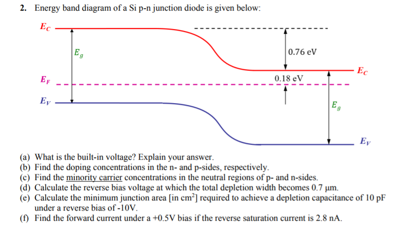
Solved 2 Energy Band Diagram Of A Si P N Junction Diode Is Chegg Com

Unit Iii Semiconductor Diodes What Are Semiconductors Semiconductors Are Substances That Conduct Electricity Under Certain Conditions I E They Require Ppt Download